Business
Electronics 3D Printer
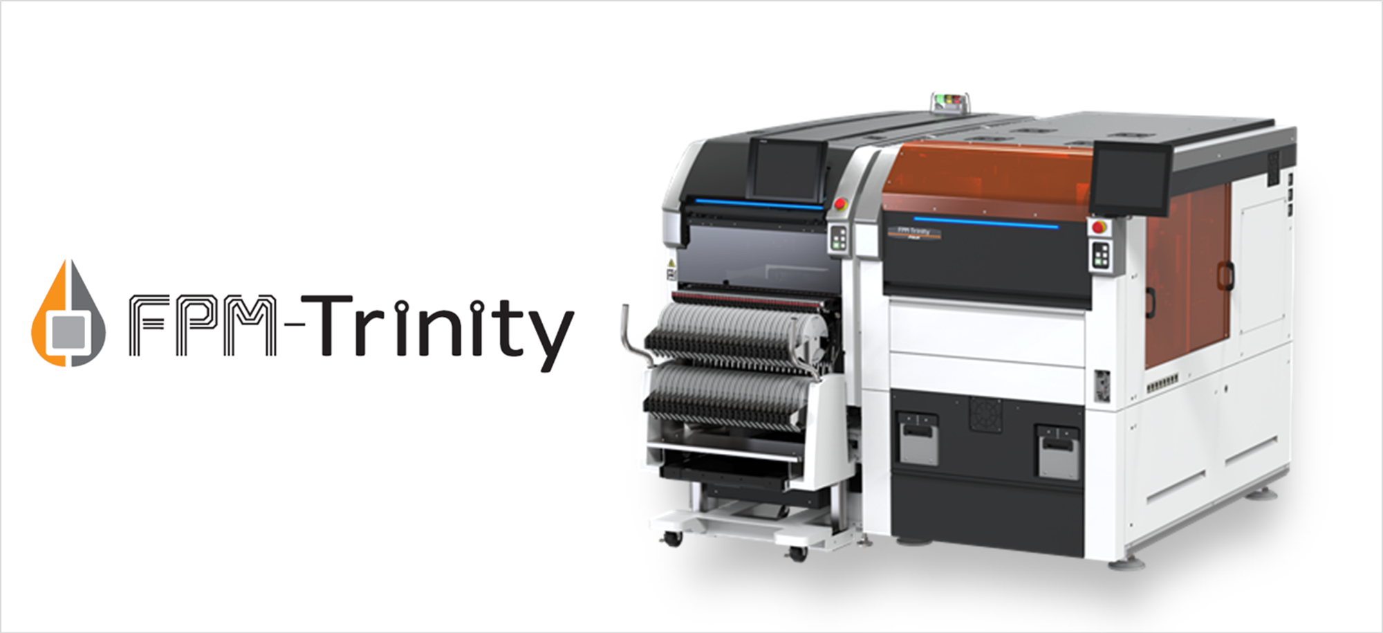
What is FPM-Trinity?
FPM-Trinity, currently under development, is the world's first machine capable of manufacturing electronic devices by combining three functions: Resin 3D formation, electric circuit printing, and electric parts placement.
By inputting design data and materials, the system can fully automate the production of panels with mounted electronic parts.
◆Manufacturing with overwhelming speed
FPM-Trinity utilizes the full additive process, eliminating the need to prepare masks and jigs for manufacturing.
Electronic devices can be manufactured in a single day, accelerating prototyping.
◆Realizes a variety of designs
The manufacturing process in conjunction with 3D data reproduces devices in ideal shapes that could not be made using ordinary electronic panels.。
◆Contributing to a sustainable society
It is a green process that reduces liquid and material waste by more than 95% compared to typical PCB panel manufacturing.
If you are interested in our prototyping services and the machine, please feel free to contact us.
We provide prototyping services for electronic modules using FPM-Trinity.
This is recommended for people who want to perform the following.
☞ Want to create electronic modules suitable for the application and installation space
☞ Want to accelerate the development cycle with short turnaround times and low-cost prototyping
☞ Want to create a one-of-a-kind custom product.
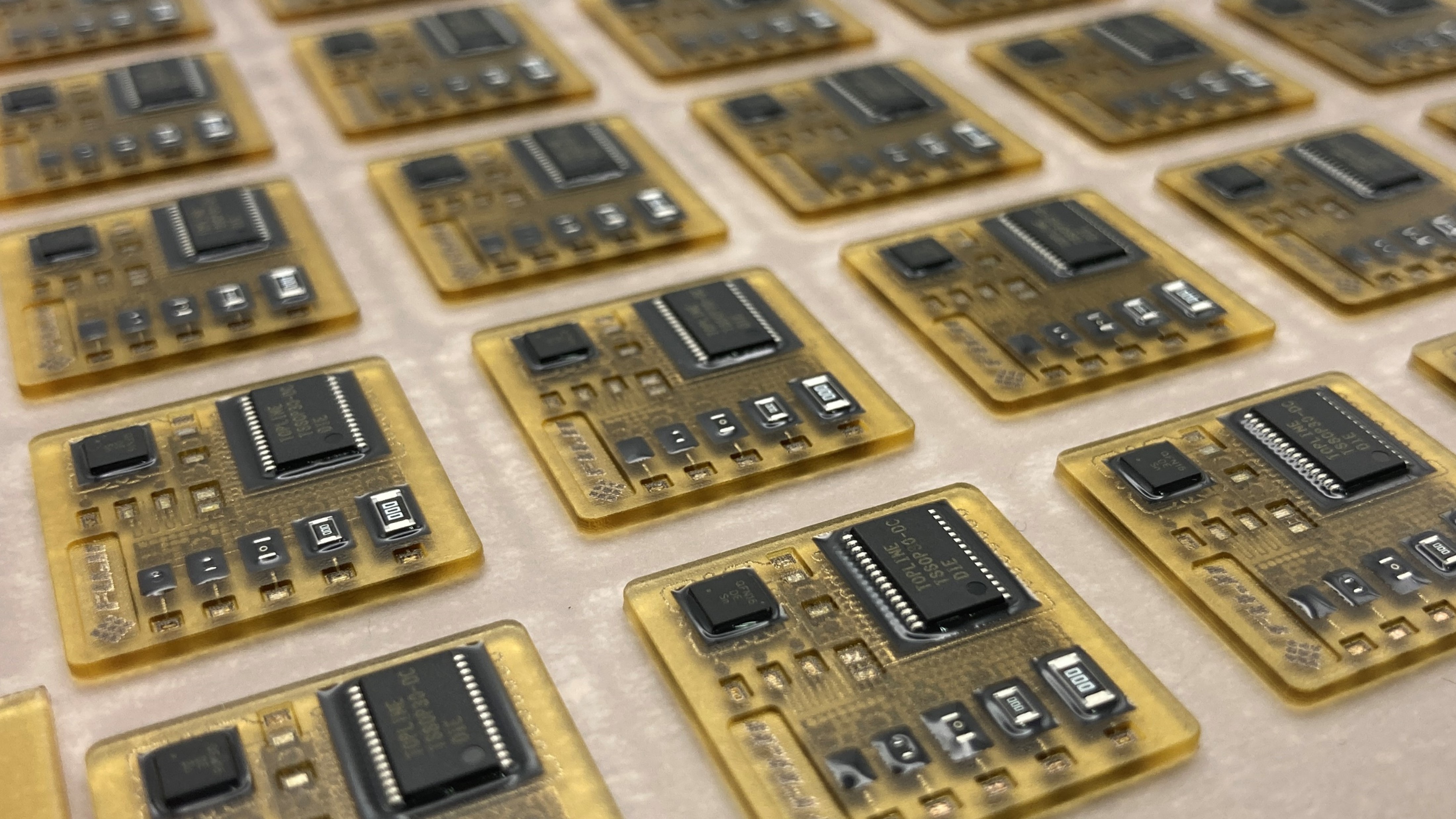
◆Case study examples
Click an image to see details.
-
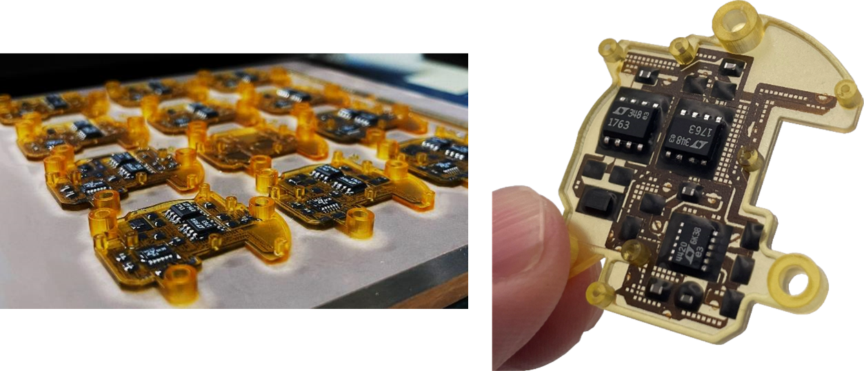
Robot power board
-
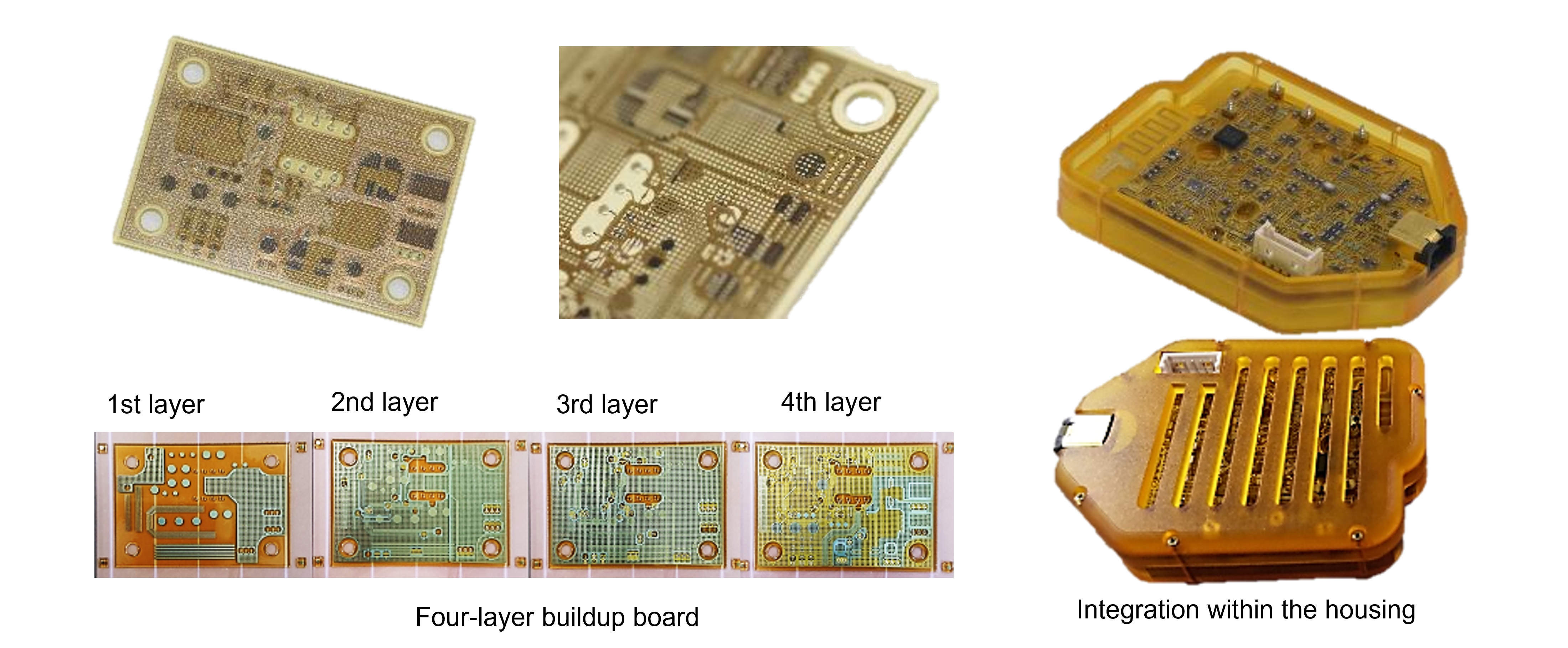
Multi-layer buildup board
-
Heart rate visualization earring
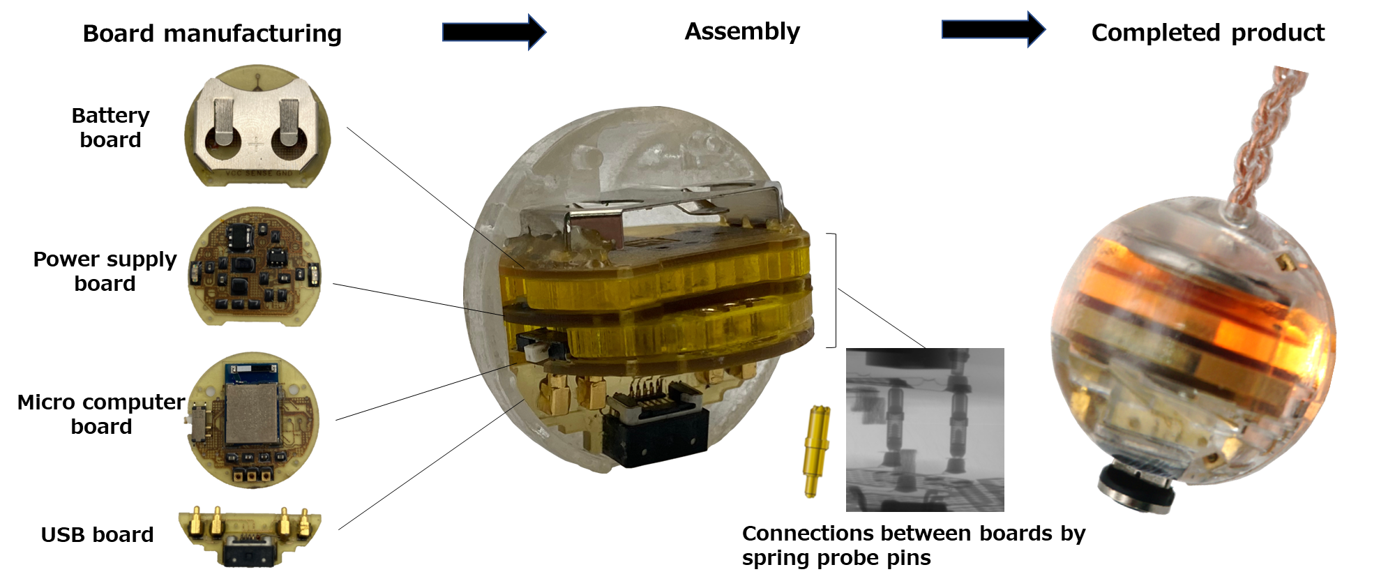
Robot power board by FPM-Trinity
- Prototype power supply boards for a custom robot were created.
- The part layout and board shape are designed to match the installation location, and the spacers required for installing are manufactured all together.
- Special shaped boards can be easily manufactured with less waste in order to reduce weight.
Four-layer buildup board by FPM-Trinity
- The four-layer buildup boards are manufactured by 3D printing.
- By designing and modeling the housing together with the boards, it is possible to make a prototype that is based on the image of the final product.
Heart rate detection earring by FPM-Trinity (Nexstar - A. Yamamoto)
- A prototype was built to demonstrate the wearable "e-lamp.", which detects the heartbeat and visualizes it with light.
- The device is reproduced in an ideal form in combination with an existing 3D printed housing.
- It allows product development to be accelerated because it is possible to easily materialize concepts.
Guidelines for design rules
| Item | Specifications(as of June 2023) | |
|---|---|---|
| Material | Resin | UV curable (orange clear type) |
| Circuits | Silver nano particle ink | |
| Component connections, electrodes | Silver conductive paste | |
| Component securing | Epoxy adhesive (black color) | |
| Resin formation | Max resin build size | 120 x 60 x 4 mm |
| Circuit formation | Trace width | Minimum: 140 um, Maximum: 1,000 um |
| Maximum layer count | 5 | |
| Layer interconnections | Blind vias (non-stacking) | |
| Part placement | Placement method | SMD |
| Chip size | 1005 (0402") to 2316 (1206") mm | |
| Package parts size (QFN, QFP, SOP) |
Maximum size: 7 mm Maximum thickness: 1 mm |
|
| Minimum electrode pitch | 0.5mm | |
| Electrode surface finish | Sn, Au |