Technology Showcase
-
#01Printed circuits using metal nano-ink
-
#023D printing with high-heat-resistant UV resin
-
#03Vias in additive manufacturing
-
#04Wiring formation and
3D printed molds on PCBs -
#05Ultra-low temperature SMT at 80 degrees C
-
#063D forming and embedded parts
-
#073D multi-layered embedding of parts
-
#08PCB connections using AM interposers
Printed Circuits Using Metal Nano-Ink
Technology overview
- Circuits are formed by directly printing nano-ink
- A resistance of 7 uΩcm has been obtained a through optimization of sintering conditions
Key benefits
- On-demand manufacturing of electronic circuits
- Pattern formation on soft materials
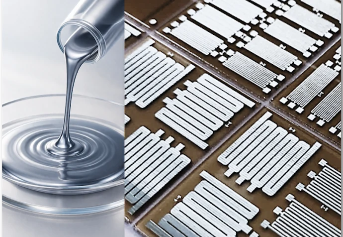
3D Printing with High-Heat-Resistant UV Resin
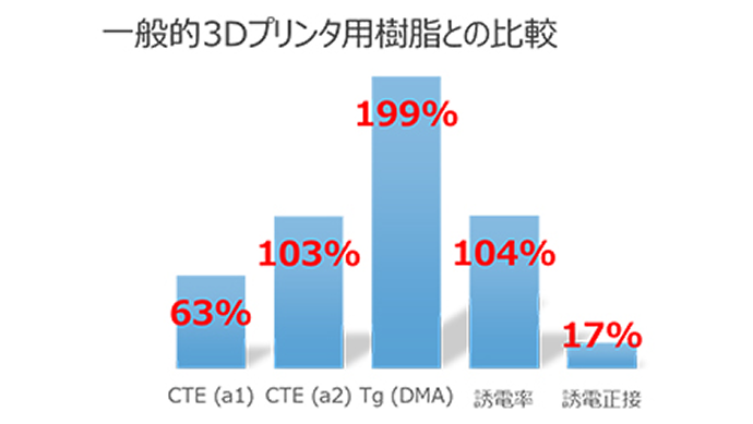
Technology overview
- Industry-leading heat-resistant inkjet ink developed in collaboration with material manufacturers
- High-resolution printing when combined with a 600 DPI inkjet printer
Key benefits
- Integration with thermal processes for printed panels (low-melting-point solder, printed circuits, etc.)
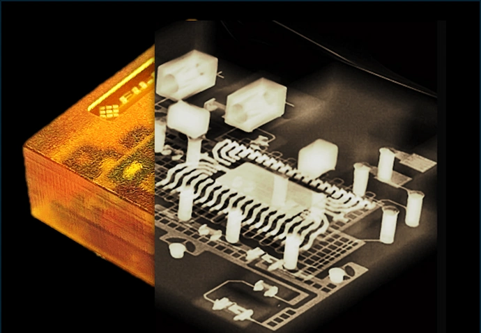
Vias in Additive Manufacturing
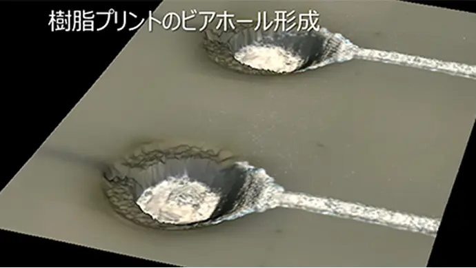
Technology overview
- Form via openings (φ0.8 mm) using UV resin inkjet printing
- Electrical connections between layers are established by printing silver ink onto the via walls
Key benefits
- Creation of all-additive build-up circuits
Wiring Formation and 3D Printed Molds on PCBs
Technology overview
- 3D printing is used to form high-resolution, heat-resistant resin on PCBs
Key benefits
- Selective molding of PCBs with directional sensors or optical components
- For interposer PoP structures and chassis mounting
Ultra-Low Temperature SMT at 80 Degrees C
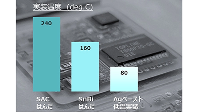
Technology overview
- Ultra-low-temperature placement using low-temperature-curing silver paste and underfill
- Maskless process for digital bump formation with a dispenser
Key benefits
- For placing parts on resins or soft materials with low heat resistance
- For processes that require additional placements at temperatures below the melting point after applying solder paste
3D Forming and Embedded Parts
Technology overview
- Encapsulation of ink-printed circuits and surface mounted parts within high-precision resin parts
- Highly controlled shapes achieved through an embedding process that eliminates irregularities in internal parts
Key benefits
- Manufacturing of electromechanical devices with design and customization features
- Waterproof applications utilizing a fully sealed structure
3D Multi-Layered Embedding of Parts
Technology overview
- 3D layout of circuits and parts by continuously embedding parts
- Fully sealed using high-precision resin 3D printing
Key benefits
- Miniaturization of devices
- Waterproof applications utilizing a fully sealed structure
PCB Connections Using AM Interposers
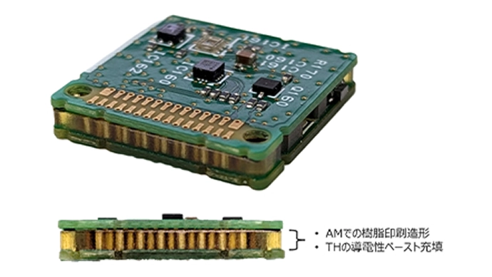
Technology overview
- Joining rigid and flexible panels using AME technology
- High-density 3D part placement while maintaining part density
Key benefits
- Miniaturization of wearable devices
- Simplifies the manufacturing of devices such as rigid-flex circuits, which are complex to assemble
Seeking Co-development Partners
We are also seeking companies interested in collaborating with us to develop applications that leverage our technologies. Ideas that were difficult to realize using conventional manufacturing methods can now be brought to life with greater creative freedom through additive manufacturing.
If you are interested in our technologies or applications, please contact us.


Facing challenges drives the future.
DNA that never stops evolving.
Human stories woven through technology.